Optical Experiments on Semiconductors
1. Absorption
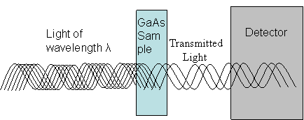
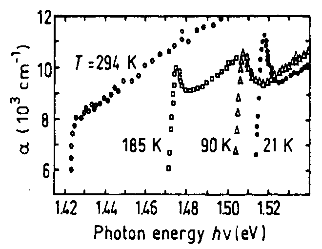
One method of determining the properties of a given sample, especially a semiconductor's bandgap, is to look at its photon absorption at varying energies of light. In a basic absorption experiment, light is incident on one side of the sample with a detector on the opposite side to measure the intensity of the light exiting the sample in comparison to the incident beam (see Figure 2.1). Absorption does not occur until the light is of a sufficient energy to allow the electron to jump the energy gap between the valence and conduction bands. Nonradiative transitions between energy levels are also possible if the energy is carried away by phonons (vibrations in the material's lattice). For an absorption vs. energy graph for GaAs, see Figure 2.2. The sharp rise in the graph near 1.51 eV for the 21 K data is indicative of the energy gap in GaAs. Only light that can cause transitions into excited states will be absorbed.
2. Reflection
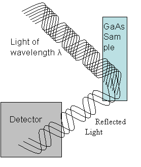
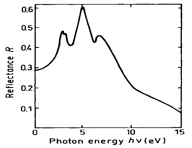
Similar to absorption measurements are reflection experiments. Light is again incident on the sample, but the detector is situated on the same side as the light source and positioned at the same angle with respect to the surface (see Figure 2.3). The energy of the photons is then varied while the reflected light intensity is monitored. See Figure 2.4 for a reflectance vs. energy graph for GaAs. Analysis of a reflectance graph is useful in determining the band structure of the semiconductor. Changes to the band structure (and transitions) due to various doping levels can be understood by comparing reflectance graphs for each concentration of doping.
3. Photoluminescence
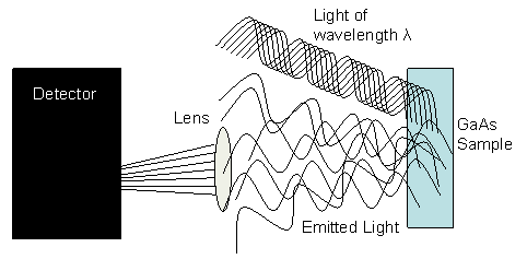 Figure 2.5. Detection by photoluminescence.
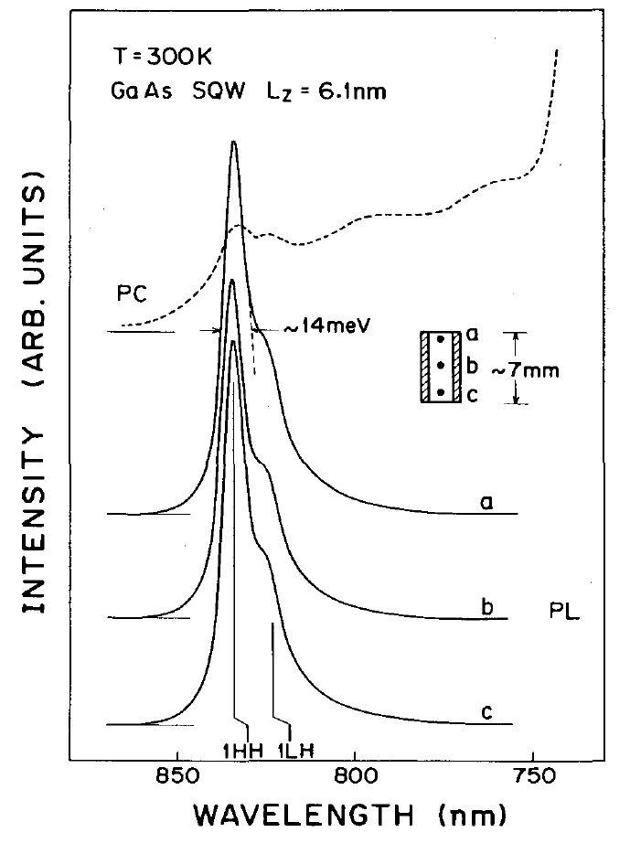 Figure 2.6. Photoluminescence (solid curves) of 3 GaAs single quantum wells at 300K. K. Fujiwara et. al. Appl. Phys. Lett. 53, 675-677.
Photoluminescence is a useful experiment for the study of semiconductors as it may be used to determine its band gap. Light of a fixed wavelength is absorbed by electrons in the sample. The energy is radiated in all directions as the electrons drop to a lower energy state. Part of the emitted light is focused by a lens and fed into a spectrometer (see Figure 2.5). The relative intensity of the emitted light is measured as the wavelength analyzed by the spectrometer is varied. P.L. differs from absorption and reflection since it measures the light that is reradiated by the sample at various energies instead of catching the main reflected beam. A typical graph of emitted light intensity as a function of incident light wavelength is shown for GaAs in Figure 2.6.
4. Photoluminescence Excitation (P.L.E.)
PLE uses the same experimental set-up as photoluminescence (see Figure 2.7), except the wavelength of the spectrometer is set to measure a fixed wavelength (usually the one corresponding to the energy gap) while the energy of the incident light is varied. In Figure 2.2 the first "bump" in the intensity is due to the formation of excitons, which form at a lower energy than that required for an electron to jump to the conduction band.
5. Kerr Rotation
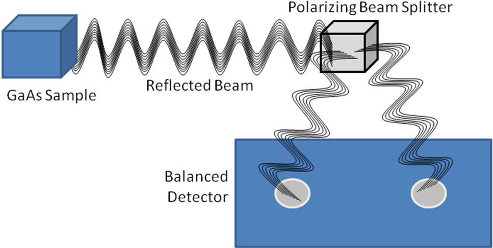 Figure 2.8. Detection by Kerr Rotation.
 Figure 2.9. GaAs electron spin resonance detected via Kerr Rotation.
For this experiment, linearly polarized light is incident on a magnetized material. The magnetization must have a component that is parallel to the direction of propagation of the light for the effect to be observed. The plane of polarization of the reflected light is different from that of the incident light after interacting with the sample as measured by a balanced detector. It differs from the Faraday effect since it measures the reflected light rather than the transmitted light (see Figure 2.8). Kerr rotation is useful for the detection of the coherence of electron spin since the changing spin will cause changes in the polarization of the incident light that can be measured over any time interval (see Figure 2.9).
6. Spin Lifetimes
The spin dynamics of a system are often described using one of three common lifetimes, labeled T1, T2, and T2*. T1 is the "longitudinal" or "spin flip" time, describing how fast spins flip their direction parallel or anti-parallel to an applied magnetic field. The energy level splitting is: ΔE = gμBB, where μB is the Bohr magneton and g is the electron g-factor for the particular material. Changing the direction of a spin in the presence of a magnetic field requires addition or subtraction of some energy; consequently T1 is typically the longest of the three times for a given material.
T2 is the "spin coherence" or "spin dephasing" time, which describes the coherence of an ensemble of spins. The decoherence described by T2 sets the time scale for potential quantum computing—many calculations will need to be done within the T2 time of the quantum computing material. T2 is also called the transverse relaxation time and is typically the most difficult of the three times to quantify. Because there is no energy difference in the transverse direction, T2 is typically shorter than T1.
T2* is the "inhomogeneous dephasing" time. It describes the apparent dephasing produced by inhomogeneous effects in the material. If the spins behave slightly differently in different places in a material (e.g. have slightly different g-factors), they get out of phase with each other. This is independent of, and cumulative with, the effects which produce T2-type decoherence; thus this is the shortest spin lifetime. Inhomogeneous effects can be compensated for through special techniques such as the spin echo, but if no such techniques are employed, T2* will be measured instead of T2. T2* provides a lower bound for T2.
For more information, please see this discussion of semiconductor spin lifetimes and decoherence by Michael Flatté at the University of Iowa.
7. Optical Study of Spin
In most III-V semiconductors, the spin states are connected to optical transitions via selection rules. This allows one to study the spins in these materials via optics: optically exciting the spins into desired states and/or detecting the state of the spins by measuring optical properties. In the important material GaAs, for example, spin coherence properties have been studied through the following optical methods (not an exhaustive list):
(a) The Hanle effect. This is a method of finding the T2* spin lifetime by measuring the depolarization of luminescence in a transverse magnetic field. In this technique the spins are oriented using circularly polarized light and their states are monitored via the polarization of the emitted light. As the field is increased from zero, the spins precess away from their initial direction, which causes the emitted light's polarization to change. The T2* lifetime is deduced from the width of the depolarization vs. field curve.
(b) Time-resolved Faraday or Kerr rotation. This is also a measurement of spin precession, typically done at higher fields, which like the Hanle effect can yield T2* spin lifetimes. In this technique, the sample is typically excited with a short pump beam of circularly polarized light, after which the spin states are monitored via the Faraday or Kerr effects acting on a linearly polarized probe beam. The Faraday (for transmitted light) and Kerr (for reflected light) effects cause the probe beam's angle of polarization to change in response to the overall spin polarization of the electrons in the sample. The precession of spins due to a transverse external field can be seen directly as oscillations in the Faraday rotation as one varies the time delay between pump and probe beams.
(c) Time-resolved decay of polarization. This is a measurement of spin decay that yields T1. In this technique, spins are first injected parallel to an external magnetic field through an optical pump pulse. The state of the spins some time later is measured by an optical probe pulse. The change in spin states between the two pulses is due to spin flip events, and the spin polarization decays according to the spin flip time.
When applied to n-type bulk GaAs samples, these optical techniques have resulted in experimental measurements ranging from 5-200 ns for T2*, and 0.04-20 μs for T1, depending on details such as sample doping level, temperature, and magnitude of external magnetic field. Overall these values agree fairly well with spin properties measured through other methods and those predicted theoretically.
8. Combined Optical/Microwave Techniques
Traditional microwave experiments detect the absorbed microwave power; these experiments are not feasible in nanostructures because there are not enough spins in the material to produce a measureable effect. However, microwave resonance can be combined with optical detection to dramatically increase the sensitivity of spin resonance experiments. This technique, called "optically detected magnetic resonance" (ODMR) has been successfully applied to semiconductors for many years. Under the proper conditions, optical detection schemes can even allow one to detect the state of individual spins, as has been done with the NV-center defect in diamond.
Further reading
For more information on optical experiments, see N. Peyghambarian, Introduction to semiconductor optics (Prentice Hall, 1993).